← Megelli 250R Wiring Diagram: Keep Your Motorcycle Running Smoothly! Basic turn signal wiring diagram motorcycle 545RFE Transmission Wiring Diagram: Simplifying Your Car Setup Dodge 545rfe transmission diagram →
If you are looking for PCI Express 设计指南(PCB板) - jinzi - 博客园 you've came to the right place. We have 25 Images about PCI Express 设计指南(PCB板) - jinzi - 博客园 like PCIe in PCB Design: Layout and Routing Guidelines | Blog | Altium Designer, PC & PCI cards - Engineering Technical - PCBway and also Review of Server PCB Layout & Schematic - Part 4: PCI Express (PCIE. Read more:
PCI Express 设计指南(PCB板) - Jinzi - 博客园
 www.cnblogs.com
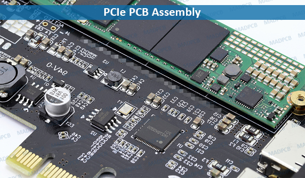
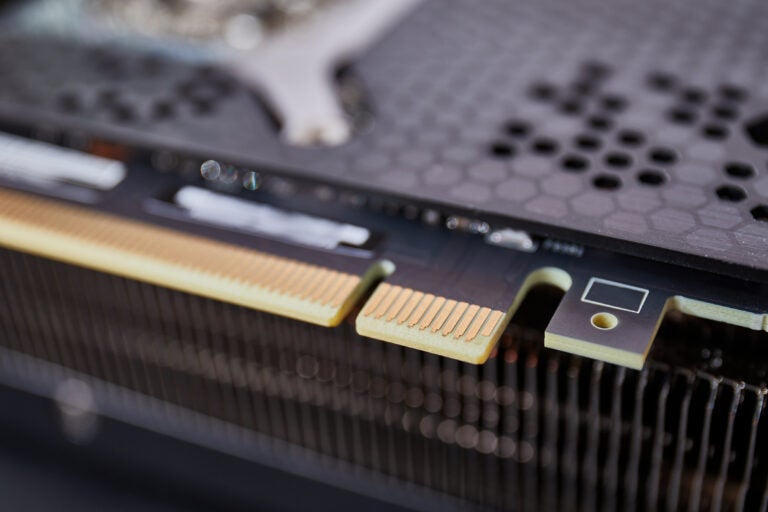
PC & PCI Cards - Engineering Technical - PCBway
 www.pcbway.com
pci card pcb pc cards design pcbway circuit board boards multi bevelling
PCB Layout Guidelines For A Successful Design
 reversepcb.com
PCIe Gen 6: PCB Design Essentials | EMA Design Automation
 www.ema-eda.com
PCIe Gen 6: PCB Design Essentials | EMA Design Automation
 www.ema-eda.com
How To Design A PCB Layout: A Comprehensive Guide
 www.wevolver.com
PCIe Gen 6: PCB Design Essentials | EMA Design Automation
 www.ema-eda.com
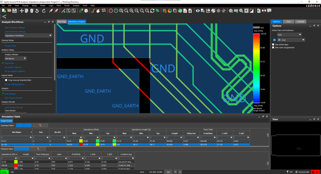
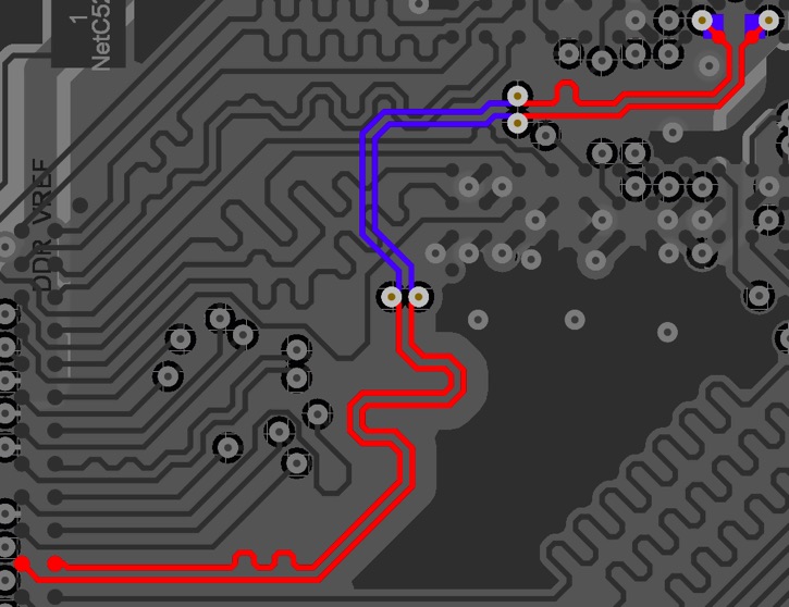
PCIe Routing Guidelines: Overview | EMA Design Automation
 www.ema-eda.com
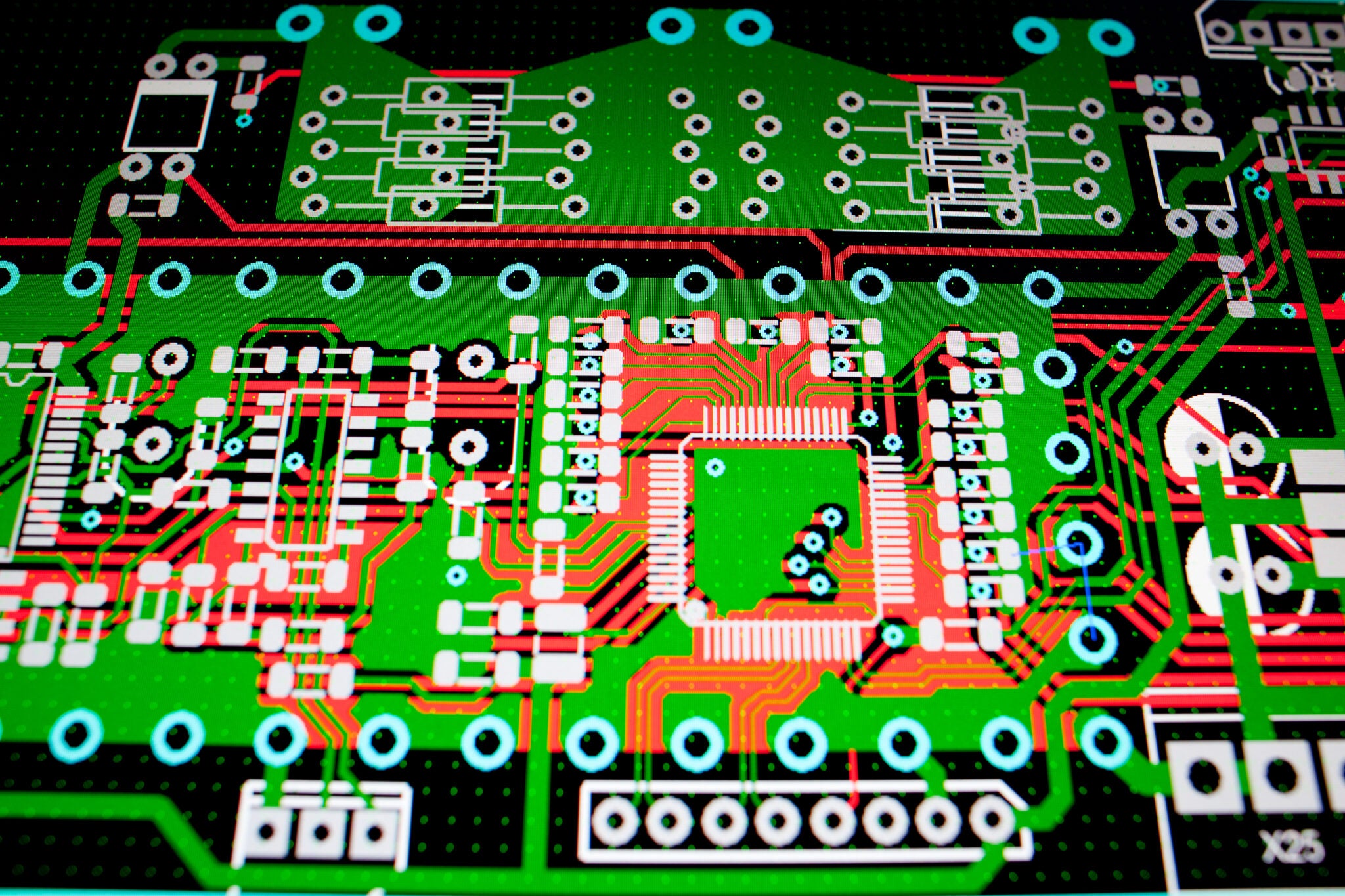
PCIE-PCB设计规范!(建议收藏)-CSDN博客
Pcie Pcb Routing Rules - PCB Designs
 pcbdesignsdl.blogspot.com
PCB Layout Design Guidelines For Switch Mode Power Supply (SMPS) Circuits
 circuitdigest.com
pcb loop short design layout supply power switch mode circuits output example above
PCB Layout Guidelines For High Speed Applications - HardwareBee
 hardwarebee.com
pcb guidelines process applications b4y
PCIE转接板 - PCB设计案例 - 通泰电子
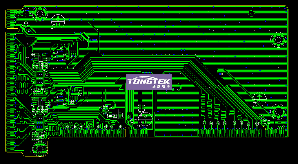 www.tontektech.com
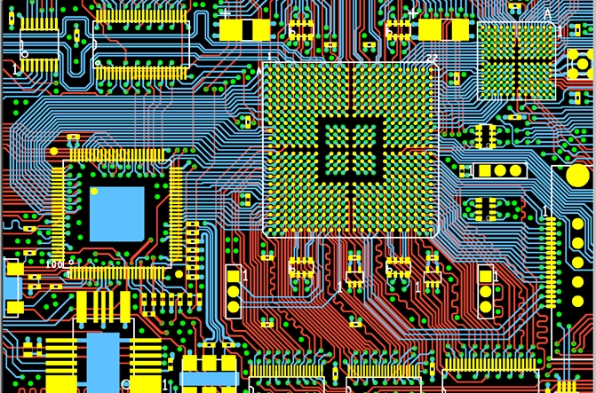
Review Of Server PCB Layout & Schematic - Part 4: PCI Express (PCIE
 www.youtube.com
pcb layout pcie pci server schematic express
PCIe In PCB Design: Layout And Routing Guidelines | Blog | Altium Designer
Pcb Layout Guidelines Smps Pcb Layout Guidelines In Altium Designer
 circuitschematics.z20.web.core.windows.net
Main Design Guidelines & Layout Rules On High Speed PCB
 www.integrasources.com
Designing PCIe Interfaces And Extenders « Adafruit Industries – Makers
 blog.adafruit.com
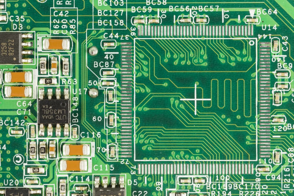
PCB Design Layout Guidelines For Engineers | Advanced PCB Design Blog
 resources.pcb.cadence.com
18 PCB Layout Tips For Improving Your PCB Design And Reducing
 camptechii.com
pcb design layout trace tips spacing traces headaches manufacturing board copper out side ground each pads between pattern using opposite
PCIe Routing Guidelines & Best Practices - Free Online PCB CAD Library
 www.ultralibrarian.com
PCIe In PCB Design: Layout And Routing Guidelines | Blog | Altium Designer
 resources.altium.com
Pcie Pcb Routing Rules Pcb Designs – Otosection
 www.otosection.com
PCB Layout Rules For PCIE, SATA, LAN, LVDS, USB, SDVO,
 www.fedevel.com
PCIe Gen 6: PCB Design Essentials | EMA Design Automation
 www.ema-eda.com
Pcb guidelines process applications b4y. Pcb layout rules for pcie, sata, lan, lvds, usb, sdvo,. Pcb loop short design layout supply power switch mode circuits output example above